
Expert Interview: Nano Dimension Co-Founder Simon Fried on the Rise of 3D Printing for Electronics


[caption id="attachment_6914" align="alignright" width="250"]

Simon Fried, Nano Dimension Co-Founder and President[/caption]The world of electronics is a young yet burgeoning area for 3D printing. From drones and satellites to laptops and smartphones, electronic devices are playing an ever-greater role in our lives. However, to operate, these devices depend on electronic components such as printed circuit boards (PCBs), antennas and sensors. 3D printing is redefining the way these components have traditionally been designed in part by providing faster product development and greater design complexity, most notably in the area of non-planar (i.e. non-flat) geometries. Nano Dimension is a company leading the field of additive manufacturing for printed electronics. Founded in 2012, the Israeli-based company has developed its own technology — the DragonFly Pro System — that can simultaneously 3D print metals and dielectric polymers. Using the technology, companies are able to 3D print prototypes in-house, faster and at a lower cost. In this week’s Expert Interview, we spoke with Simon Fried, the Co-Founder and President of Nano Dimension, to discuss the rise of 3D printing for electronics and how Nano Dimension is paving the way for this unique application.Can you tell us a bit about Nano Dimension?Nano Dimension exclusively offers additive manufacturing for electronics. Previously, electrical engineers haven’t had the luxury of being able to test out an idea by using 3D printing. Additionally, the concerns faced by electrical engineers today — such as the huge amount of planning and outsourcing to third parties — can be dealt with by being able to 3D print electrical circuits. So our solution offers the freedom, flexibility, secrecy and general practicality that 3D printing provides within the mechanical context and bringing it to electronics. That’s one aspect. Speaking specifically about your DragonFly Pro System technology, could you touch more on the value it brings to the table?Sure — imagine you’re an electrical engineer who needs to design the next PCB (circuit board) for your employer’s next product. The first thing you have to do is work out what needs to work in the product and what the right components and sensors are to use. That’s typically how a board is designed. And this is done using EDA (Electronic Design Automation) software — essentially, you’re using sophisticated design software and often also doing a lot of simulation before sending your design out to a third party manufacturer. What Nano Dimension allows electrical engineers to do through our technology is to design and additively manufacture a physical board to ensure that’s it’s been designed correctly and see if there are any errors, oversights or opportunities for improvement. This is instead of having to obtain a purchase order or get a third party to manufacture the board, which could take as long as several weeks depending on the complexity of the design and the availability of the supplier. With our technology, you’re able to go from having your idea to printing it in about a day. We’ve had customers that have been able to achieve 6 weeks of work in a day and a half because they were able to print boards for testing themselves instead of waiting for third party suppliers to deliver them.
By eliminating the middleman when it comes to prototyping, we enable companies to take more risks when designing. Designers are able to test more ideas more frequently and also to develop and test in secrecy. If you can develop quickly and cheaply, then the cost of failure is brought down, which means people aren’t afraid of innovating.
One of the reasons a lot of defence companies have been in touch with us is precisely because they’re often very constrained with regards to which designs they can send out and to which supplier. They think long and hard before they send anything out to a third party — and sometimes they’re just not allowed to. So our technology allows you to do many of the same things that additive manufacturing allows you to do in the mechanical context but in the context of electronics.What other benefits does additive manufacturing offer electronics?
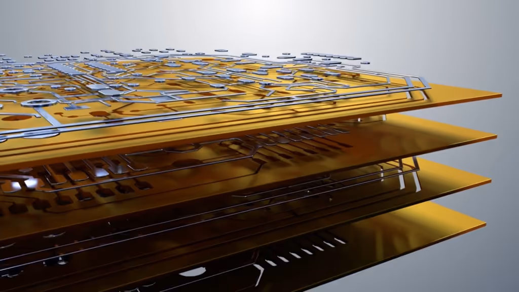
Additive manufacturing allows you to make shapes and geometries that are not possible to make any other way. For an electrical engineer, who’s used to working in a very binary environment, all planar with either vertical or horizontal signal traces, that’s amazing.
The world of electronics is a lot less forgiving than say a mechanical engineer’s task, where you can solve a problem in many different ways and there are not that many constraints. Electronics doesn’t have any of those degrees of freedom — it’s very precisely defined by the traditional manufacturing process and the components that you plan to use. So you’re in a straitjacket when it comes to how you can design and manufacture.With additive, you open up a whole host of new design opportunities for electrical engineers who are suddenly able to make things that have vastly different and non-planar geometries, as there are now far fewer constraints regarding how you go about designing things. Until now, it’s never occurred to people to design differently because they couldn’t make differently. For us, it’s a two-pronged approach: one is that you want to let people make the traditional PCB and RF electronics that they make today but more effectively, efficiently and independently. But we also want to allow people to start making different things, not just making things differently. That’s the vision of what we’re doing, change the manufacturing process, make it something that can be done in-house and with far greater design freedom as a result. What are some of the challenges involved in 3D printing electronics?It’s very complex additive manufacturing because we’re printing metals and polymers at the same time. Metals are best printed at elevated temperatures and have their own set of requirements for successful printing, which is usually very distinct to what’s good for polymers. This means there are a lot of material, process and resolution challenges when we are trying to get metals and polymers to get along with one another — which they typically don’t want to do.We’re focused on printing both functional materials, simultaneously and at very high resolutions. What’s the current state of electronics 3D printing market?
The whole area of 3D-printed electronics is a young space. There aren’t many companies that are active within it. But what we’re seeing is that the space is evolving in quite a similar way to how traditional additive manufacturing evolved and the early adopters of this new technology are oftentimes the same companies that dipped their toes in the water of traditional 3D printing perhaps 10 years ago.
The leaders in additive manufacturing adoption are the same kind of industries that are now making strides in the direction of additive electronics. So that’s the aerospace, defence and R&D organisations which are rushing to adopt the systems. So 3D-printed electronics is an exciting new technology and the most forward-looking companies or those with significant R&D needs are adopting it. How do you see additive manufacturing evolving for electronics in the coming years?The landscape is really exciting. What we’re seeing is that the world of mechanical and the world of electrical are getting ever closer. A key part of that journey is the mechanical design software, like Autodesk, Solid Edge and SolidWorks. Most of those companies are moving towards offering electrical design software as well. So the designer will be able to design electronic and mechanical parts in a more integrated way. If we consider the kinds of products we’ll see in the future, what everybody ideally would have in their products or in factories are designs that elegantly merge the mechanical needs with the electrically functional, such as communication or computational, needs.With flexible phones for example, we see that the mechanical properties are evolving rapidly, which means that the electrical capabilities also have to evolve alongside. And we can look at things like wearables — trying to get wearables to include electrical traces, which is very difficult. A lot of the wearables today are not yet delivering on form-factors that are optimal.So whether it’s is wearables or other products, these worlds of mechanical and electrical are getting ever closer to each other. They have to do more things one alongside the other. Ultimately they have to adapt to the goals and needs of any customers or users. The IoT trend is also placing new demands on designers who are increasingly required to consider how to introduce electrical aspects into places that have historically been ‘dumb’ parts.
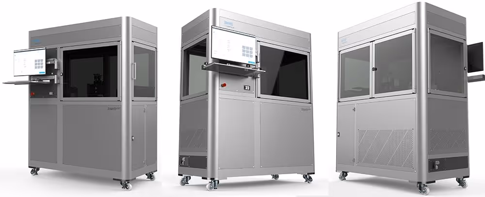
Long-term, we imagine that 3D printers will be printing ever higher proportions of final products, including what is currently being done on separate machines —whether that’s on the electrical or mechanical side, the assembly or even aesthetic such as colouring elements — all will be done in the same machines and these machines are going to be manufacturing very complicated, highly customisable products. In the short term, we believe it’s going to evolve in much the same way the mechanical additive space has evolved. Over the last ten years, people have been speaking about rapid prototyping and it was only a very select set of companies really adopting additive manufacturing technology. This was then helped a lot by people being able to access additive manufacturing through service bureaus. Now the 3D-printed electronics space is in the same position — it’s now probably where the traditional AM space was about 5 years ago. But it will catch up more quickly because there is more awareness now: electrical engineers are not coming to additive manufacturing completely clueless because they’ve seen what their mechanical colleagues have had access to and are already capable of doing. So we’ll see it becomes something that solves discrete manufacturing opportunities probably more quickly than has been the case for traditional mechanical applications. At present, it’s mainly rapid prototyping, but it could be only a few years before we see higher-volume additive manufacturing of electronics. This is because nearly all products today involve electronics: cars, personal computers, homes, telephones. And now with the advent of the Internet of Things, everything is going to speak to everything. That means most products will be electrified in one way or the other. So everything is going to communicate and maybe even compute to a certain extent. With all these trends of electronics going into places it’s just never been before, whether it’s food packaging, cars or medical devices like implants. These things are all going to change, they all are going to require better ways of making smaller things or better ways of making more complex things or better ways of making more functional things. In this day and age, those will ultimately require the electronics to adapt to new requirements. You’ve mentioned that 3D-printed electronics is still very new and there are few companies on the market. What makes Nano Dimension a market leader in this space?I don’t believe there are currently any enterprise or professional offerings for 3D-printed electronics other than what Nano Dimension has brought to market. In the same way that you have the maker community who might be using something like a Makerbot-type printer for home use, there are a couple of companies active in that area when it comes to printing electronics. But there aren’t any other solutions at the enterprise level. So what we provide is quite a unique offering, a one-stop shop for electrical engineers or companies who want to change the way in which they design, make and innovate electronics. To the best of my knowledge, they won’t find such a solution anywhere else. [caption id="attachment_6928" align="alignnone" width="840"]
Nano Dimension's DragonFly 2020 Pro 3D Printer[/caption]Nano Dimension has worked with companies in a number of different verticals. Could you give an example vertical and use case where your technology has been an asset?A key vertical has been aerospace and defence, with a great example use case being antennas. When it comes to 3D printing electronics, you can print circuit boards, antennas or parts that are both structural and electrically functional. However, antennas are a bit of a black art: when designing them, you never know exactly how they are going to work. It takes a lot of iterations and trial and error before you know you’ve made the best design that you can for that particular need. With antennas, we recently worked with a company called Harris Corporation where we achieved quite an exciting breakthrough. Harris wanted to apply the technology to antennas and testing, which wasn’t a use case we’d initially been proposing. Harris helped us to understand that this is a great solution for those who are focusing on designing antennas as well. More importantly, we found that the 3D-printed antennas performed exactly the same way as traditionally manufactured antennas.[caption id="attachment_6924" align="alignnone" width="780"]
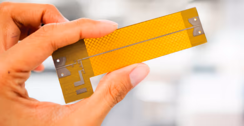
Nano Dimension and Harris Corp. partnered to produce 3D-printed RF circuits[/caption]
So antennas are one application area that is particularly relevant and it falls into that aerospace and defence vertical where low-volume manufacturing of very high complexity items is a key focus. That’s very much a sweet spot of additive manufacturing in general, where you see complexity and low volume.
If you’re looking at production volumes in the of hundreds of millions, then additive manufacturing isn’t the answer in any industry, at least not yet. But it certainly is in the aerospace niche, where there is not so much of a volume question as there is the element of reliability and solving complex problems. Why are has aerospace and defence been such a key vertical? Defence companies need to maintain a great level of secrecy. Another constraint is that they are limited in the number of suppliers that they’re allowed to work with, and their internal procedures for releasing a design file to a third party are incredibly complex. These types of companies have the combination of a need for security and low-volume manufacturing as they’re working on discrete and high-value projects. And that’s really where additive took off, in the mechanical types of application as well. So we are following suit in terms of discovering where the application happens first. Are there challenges when it comes to designing 3D-printed electronics?
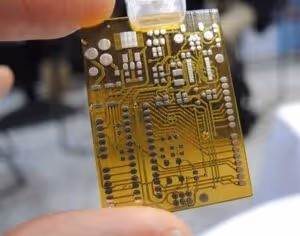
If you want to use our technology to make a traditional green printed circuit board (PCB), one that is square or rectangular and flat, that is the space where you have electronic design automation software.You have CAD software in the 3D world and in the electrical world you have EDA software, which is software we can work directly with. If you use this software to design a circuit board, our software will essentially interface with traditional design software and print it out. That’s the existing flow, using existing file formats and we don’t require anybody to do anything that that hasn’t been done before. Where you do have challenges on the software side is when you start looking at what’s called non-planar electronic circuits, essentially creating circuits that are not flat. For example, instead of the green motherboard being a rectangle, it might be a pyramid or cube because that shape fits a particular space in a more optimal way.
When you look at designing 3-dimensional electronics that don’t use the traditional layered PCB flat design approach, electrical engineers today are incredibly limited. They can’t design an electrical trace that is anything other than flat because that’s the way PCBs are traditionally manufactured. And yet it could be really useful if they could design traces that were at an incline. Currently, if a designer wants to do something different, something that frees up a lot of the constraints, such as design non-planar circuitry they will have to use mechanical CAD software, which is really intended for mechanical engineers.
At the moment, while our printers are certainly able to print non-planar geometries, currently there is no EDA software around that is able to design such parts. That’s why we now see large companies like Siemens or Dassault Systèmes looking to integrate the worlds of electrical and mechanical design with their software packages. Nano Dimension has developed an add-in to SolidWorks that integrates directly to our precision 3D printing system.We’ve seen the same trajectory with traditional 3D printing as well. If we go back a decade and ask people which CAD software they were using to design full-colour parts, the software wasn’t necessarily able to facilitate such designs. Even though there were certainly printers out there able to deposit colours in ways that would have made it physically possible to print, just very difficult or perhaps impossible to design. There are things in the electrical space that are like that as well, where the printer can certainly print, but we may have to wait a few years before the features in the design software are actually developed. So the design software is catching up to the hardware?Yes, very much so. Particularly, in the non-flat area. Non-planar, new geometries require new design software which is waiting in the wings. In terms of additive manufacturing more generally, what are some of the core challenges still facing the industry?
Additive manufacturing faces the challenge of not succumbing to the second wave of hype. We all know about the big 3D printing bubble around 2010, which was driven by hype and over—expectation, with the industry getting caught up in its own narrative. And now what we're seeing is a kind of a replay of that with people using the term additive manufacturing instead of 3D printing.
So the question is will the systems really start to deliver in time for this not to be seen as yet another wave of hype? That’s a risk for everybody in the industry. Can the technology continue its transition to manufacturing?. Certainly, additive manufacturing is now much readier to play a manufacturing role, so it’s often a question of what role it will play as a business tool. It used to be just a time-compression prototyping tool but now AM is a technology for organisations to adopt just as they would any other manufacturing technology. What we are seeing is different types of additive manufacturing systems being integrated into traditional manufacturing lines. The role is shifting from the early design stages to either complementing manufacturing by producing jigs and test-fixtures or by actually producing final parts.On top of that, the additive manufacturing industry definitely needs solutions to more materials. 3D printing is theoretically capable of producing parts of high complexity and functionality, whether it’s mechanical, biological, electrical. But making that happen comes down to having enough material options. Polymers are getting stronger, a wider range of metals is now printable and for electronics additional functional aspects such as dielectric constants are paramount.Along with materials, there’s also the question of standards. To properly mature as an industry, you need to have standards that everybody subscribes to. You need to have processes, like ways of tracing products and ensuring IP protection for files. So for the industry, it will be less of the glitz and glamour and more of the nuts and bolts of how to deploy these technologies effectively. How confident are you that additive manufacturing won’t succumb to the second wave of hype?I have a reasonable amount of hope as more and larger companies are engaged at this time and we’re seeing actual strategies in place rather than just excitement. So I think yes, there are enough big companies and enough experienced people in the industry now, that it will rise to the occasion. So yes, it’s a big opportunity not without its challenges. I think the additive manufacturing industry will deliver on its promise. What advice would you give a company looking to adopt additive manufacturing, but doesn’t know where to start?For a company that has no or little knowledge of AM, my recommendation would be to understand that manufacturing of this type is a non-trivial consideration. It’s a complex space with many different types of printers, materials and so on. The technologies you decide to explore and try out may well not be the right ones. So one needs to be very informed of exactly what one wants to do and be prepared for a learning curve — often the engineers who get the system don’t necessarily have a deep understanding of how to deploy it. We certainly recommend people learning more, they should engage with service bureaus earlier rather than later and start to get their head around what the different technologies are and service bureaus are a phenomenal way to understand what the offerings are and how different deposition technologies and materials actually deliver to the needs of your organisation. There are a lot of opportunities and one is best served by exploring them in a methodical way and being willing to learn. So plan ahead of time, use service bureaus, understand the huge differences between the different approaches. There is no such thing as “additive manufacturing”, it’s really which material and which machine are best for your particular application. Finally, what does 2019 hold in store for Nano Dimension?We hope 2019 will be as great a year for us as 2018. While I can’t really comment on specifics, we’ll continue to launch our technology as we have been doing this year. Overall, we’re very confident that additive manufacturing of electronics will be as well received as additive manufacturing of mechanical parts — and perhaps even more so!Images courtesy of Nano Dimension.To learn more about Nano Dimension, visit: https://www.nano-di.com/


.svg)

Subscribe to our
newsletter
